Europe opens NanoIC pilot line to design the computer chips of the 2030s

Marco Ryan
- Published
- News, Technology

A new cleanroom facility in Belgium and the release of advanced design toolkits will allow researchers and start-ups across Europe to begin designing next-generation chips years before they can be physically manufactured
A major new semiconductor research facility has opened in Leuven, Belgium, giving European researchers, universities, start-ups and chip designers the ability to begin working on the technologies that will power computers, artificial intelligence systems, vehicles and data centres in the next decade.
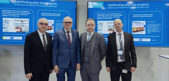
The facility forms part of the NanoIC pilot line, a European initiative led by imec and supported under the European Chips Act.
It combines a 2,000 square metre expansion of imec’s cleanroom — a highly controlled laboratory used to develop microscopic chip components — with the release of two advanced digital design toolkits that allow engineers to simulate future chip technologies long before they exist in factories.
Inside the cleanroom will be some of the most advanced chip-making equipment available, including ASML’s next-generation “High NA EUV” lithography system. Lithography is the process used to print the intricate patterns that form a chip’s circuits at scales measured in atoms.
Alongside this physical infrastructure, NanoIC has released two “process design kits”, known as PDKs. A PDK is a detailed set of digital rules, models and software files that allow designers to experiment with how a future chip technology would behave. It means designers can begin working with tomorrow’s chip structures today.
Luc Van den hove, chief executive of imec, said: “Since announcing in May 2024 that imec would host the NanoIC pilot line, we’ve moved at full speed – accelerating tool acquisition and launching a comprehensive recruitment program.
“Today, that effort culminates in the inauguration of a 2,000m² cleanroom extension at the imec premises.”
One of the toolkits is called the “A14 pathfinding PDK”. The “14 Angstrom” reference signals an extremely small scale. An angstrom is one ten-billionth of a metre. At this level, engineers are working with structures only a few dozen atoms wide.
A key feature of this design environment is something described as “direct backside contact”. In simple terms, this means supplying electrical power to a chip from the back of the wafer rather than routing it through layers of wiring on the top surface. This reduces electrical resistance, known as “IR drop”, which wastes energy and limits performance.
According to NanoIC’s data, this approach could allow future chips to be 18 per cent smaller and use 7 per cent less power for the same performance when compared with earlier designs. The toolkit is supported by industry-standard software from Cadence and Synopsys and includes a large design library to allow practical experimentation.
The second toolkit focuses on “embedded DRAM”. DRAM, or dynamic random-access memory, is normally located outside a processor and is used to temporarily store data while a computer is operating. Embedding this memory directly onto the chip brings it physically closer to the processor, reducing the time and energy needed to move data back and forth.
This is particularly important for artificial intelligence systems and data-intensive workloads, which require rapid access to large volumes of information.
Marie Garcia Bardon, department director at imec and work package leader within the NanoIC project, said: “PDKs like A14 and eDRAM are catalysts for learning and design. They offer a robust environment for hands-on evaluation and quantitative comparison of different technology choices.
“This approach accelerates learning, de-risks architectural and design innovation, and helps designers prepare for advanced logic nodes and embedded memory technologies well before hardware becomes available.”
Both PDKs are being made available through Europractice, a European access scheme that allows research institutions and companies to use advanced chip design tools. Workshops are planned in March and May to support adoption.
Giuseppe Fiorentino, programme manager for NanoIC, said: “By making these PDKs broadly accessible, we lower barriers for universities, industry, and start-ups to engage with next-generation technologies.
“Access to realistic rules and flows enables teams to explore new research directions and breakthrough concepts that will feed directly into the European semiconductor value chain.”
The NanoIC pilot line is supported by research partners in France, Germany, Finland, Ireland and Romania. Over the next five years, more than 100 new tools will be installed across these sites to support experimentation with technologies beyond the current 2 nanometre manufacturing node.
Van den hove added: “By providing access to cutting-edge semiconductor technologies, the NanoIC pilot line will play a crucial role in strengthening Europe’s industrial fabric in the AI era, and ensuring a climate of economic growth, security, and prosperity for decades to come.”
READ MORE: ‘Universe ‘should be thicker than this’, say scientists after biggest sky survey ever‘. The most detailed map of the modern cosmos yet suggests the universe is slightly less “lumpy” than Big Bang physics says it should be, raising fresh questions about dark energy, gravity and how the cosmos evolved.
Do you have news to share or expertise to contribute? The European welcomes insights from business leaders and sector specialists. Get in touch with our editorial team to find out more.
Main image: Researchers inside imec’s cleanroom facility in Leuven, where new NanoIC tools will allow designers to model next-generation chip technologies before they can be manufactured. Credit: imec
RECENT ARTICLES
-
 Firms ‘wasting AI’ by using it to speed up bad habits
 -
 AstraZeneca revives £300m UK investment after pausing major projects
 -
 UK refineries asked to maximise jet fuel supply amid Hormuz disruption
 -
 Britain must shape AI future or be left at its “mercy and whim”, Liz Kendall warns
 -
 BP profits more than double as oil price surge lifts trading business
 -
 MINI at 25 – the numbers behind the Oxford-built icon
 -
 More than half of employers say they cannot find graduates with the right AI skills, study finds
 -
 Stratospheric telecoms blimp completes “historic” record 12-day flight over Atlantic
 -
 MICE market forecast to reach $2.3tn by 2032, report says
 -
 Mobile operators warn of higher bills and slower 5G rollout after energy support exclusion
 -
 Lufthansa cuts 20,000 summer flights as Iran war drives up fuel costs
 -
 People act more rationally when they think they are dealing with AI, study finds
 -
 Toxic bosses may thrive at work, but the office pays the price, new research finds
 -
 Europe launches ‘anti-kill switch’ cloud shield as Trump fears grip Brussels
 -
 Starmer summons social media chiefs to Downing Street over child safety
 -
 The European Spring 2026 edition – out now
 -
 Inside Qantas’ new ultra-long-haul A350s with stretch zone, jet lag lighting and fewer seats
 -
 Landmark UK nuclear deal to cut reliance on foreign energy after Middle East tensions
 -
 Breitling launches £9,500 Artemis II watch as Moon crew returns to Earth
 -
 Ivy and Annabel’s owner agrees £1.4bn sale of hospitality empire to Abu Dhabi-backed buyer
 -
 Orbán concedes defeat as Péter Magyar heads for sweeping Hungary election victory
 -
 UAE unveils plans for major new military rescue training centre
 -
 Electric air taxis move closer after aircraft completes key in-flight switch
 -
 World’s largest cruise ship revealed with nine pools, 28 places to eat and giant waterpark
 -
 Artemis II crew break Apollo 13 record for farthest human spaceflight


